


Ultra-High Contrast Design Specifically For Silicon Transmission Observation: Semiconductor Internal Observation Microscope SWIR-7200A
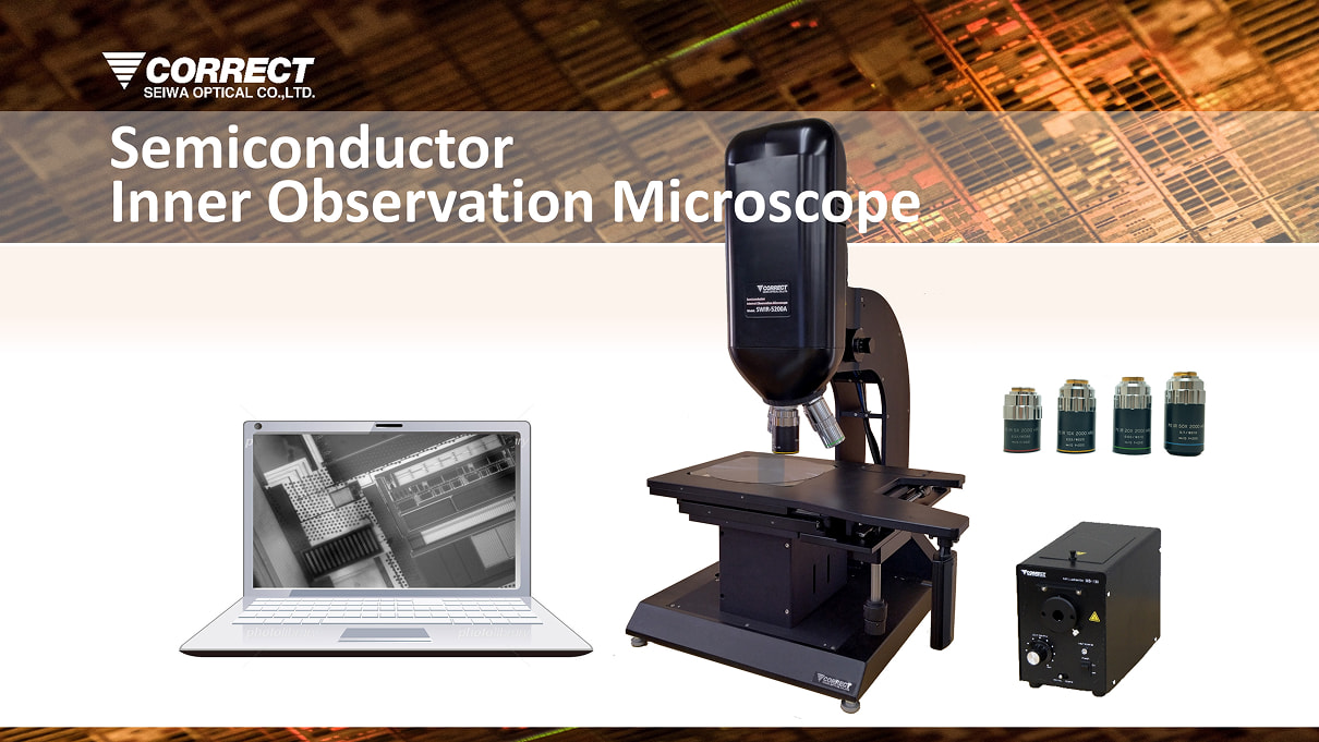
Semiconductor Internal Observation Microscope
By Blocking Visible Light, All Functions Are Concentrated Within The SWIR Range, Clearly Displaying Metal Patterns Through Silicon
The SWIR-7200A is a semiconductor internal observation microscope specifically developed for the wavelength range of 1100 to 2000 nm, which transmits through silicon, and is specifically designed for use with SWIR (InGaAs) cameras. Unlike typical near-infrared microscopes, it eliminates the ability to observe in the visible range, which is visible to the human eye. By applying a unique optical design optimized for the target wavelength and a special AR coating, we have made it possible to observe metal patterns transmitted through silicon with extremely strong contrast never seen before. With over 10 units installed in leading semiconductor manufacturers worldwide, it is chosen as a reliable tool supporting quality assurance and technological development in the field of internal inspection and defect analysis of mounted IC chips.
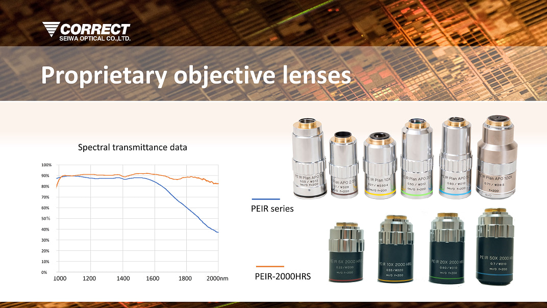
SWIR Objective Lens
Uniquely Designed Objective Lens And Specialized Technology To Correct Silicon Aberrations
This makes it possible to visualize the fine metal patterns and defects of next-generation semiconductor devices with extremely sharp resolution, regardless of the sample thickness.

Near-Infrared Halogen And LED Lighting Systems
An Ideal Near-Infrared Illumination System That Combines Wavelength Selectivity And High Brightness.

A Global Support System Connecting Parts Of The World
A Trusted Global Network Chosen By World-Class Manufacturers
- URL (Japanese): https://www.seiwaopt.co.jp/