


Wafer Plating Equipment Adopted by over 100 Research Institutions
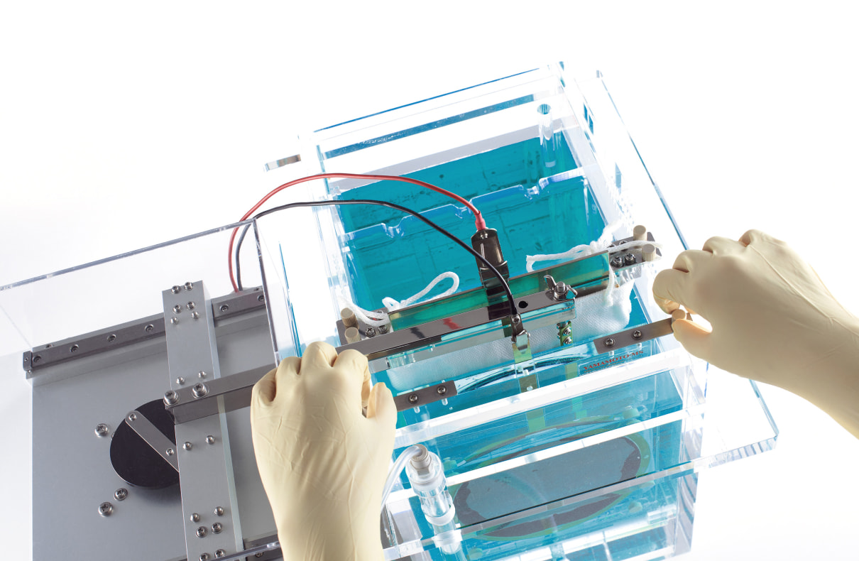
Wafer Plating Equipment Adopted by over 100 Research Institutions
We Offer Plating Equipment That Can Accommodate Wafers of Various Sizes and Shapes, from ø2 to 12 Inches.
We will propose a system including draft chamber usage if you tell us the type and bath temperature of the plating,
the size of the sample to be plated, the desired amount of plating solution and the rough specifications of the plating.
Our semiconductor plating equipment has a track record of 26 years and is used by many research institutes and manufacturers.
We can perform precision plating on silicon wafers, glass substrates, ceramic substrates,
special materials, films, etc., research on semiconductors, MEMS, LIGA, various sensors, photovoltaic power generation, aerospace industry, chemical industry, and various raw materials, etc.
We have many achievements with small-volume production equipment.
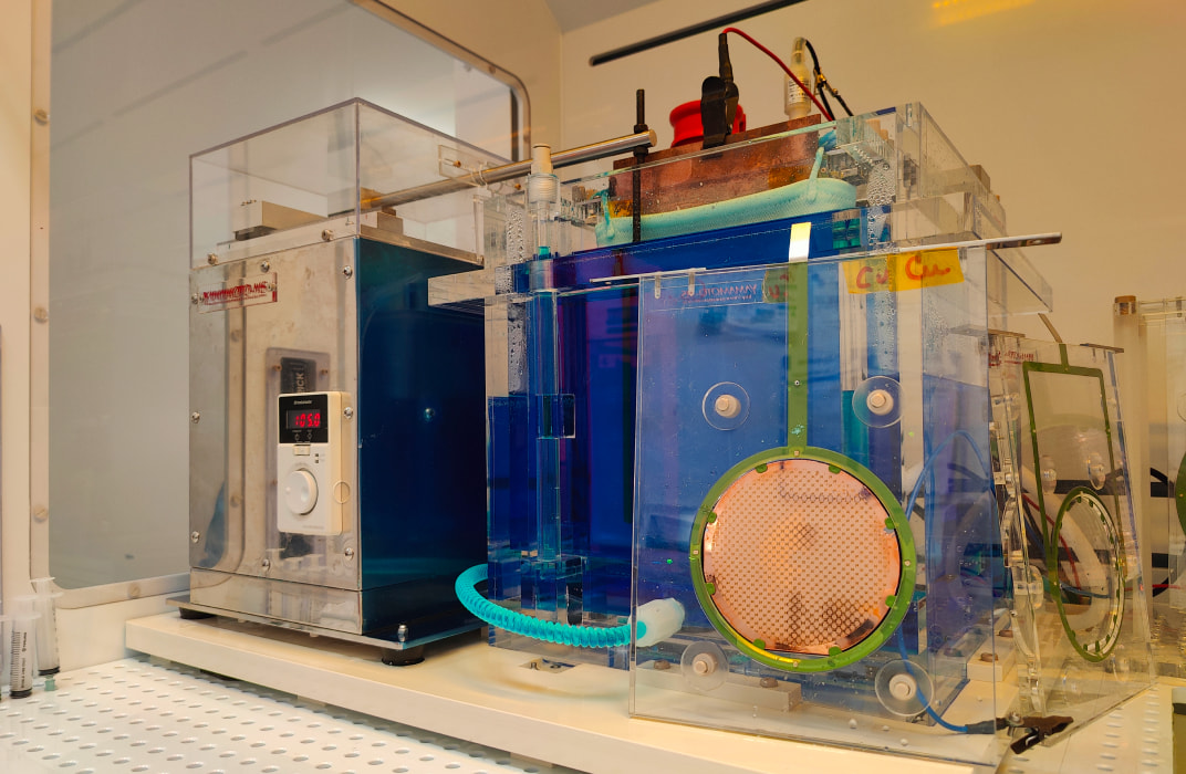
Photo Images of the Equipment and Samples after Copper Sulfate Plating. (From the LAAS laboratory at CNRS, France)
Plating with a Film Thickness Distribution of ±3-5% or Less Is Possible.
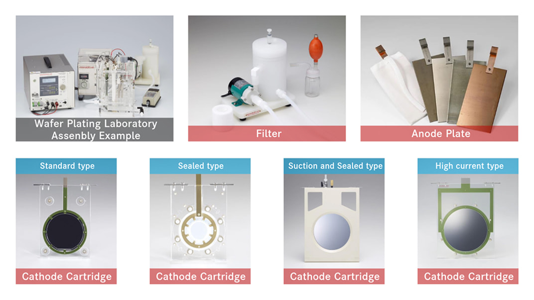
A Complete Set of Wafer Plating System.
Experiments Can Be Conducted under Various Conditions.
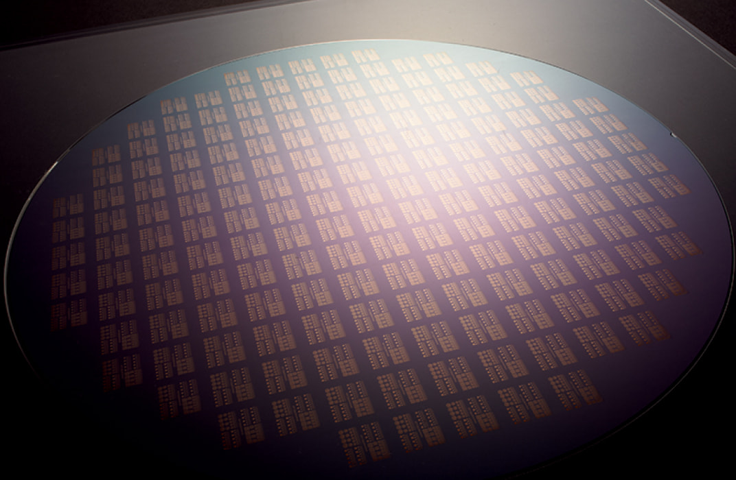
Photo Images of a Silicon Wafer
Both Available Domestically and Internationally
- URL (Japanese): https://www.yamamoto-ms.co.jp
- URL (English): https://www.yamamoto-ms.co.jp/en